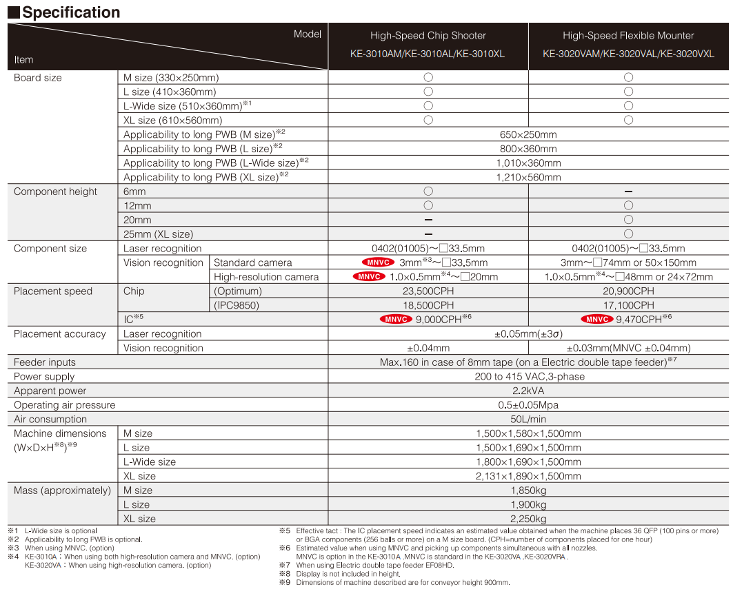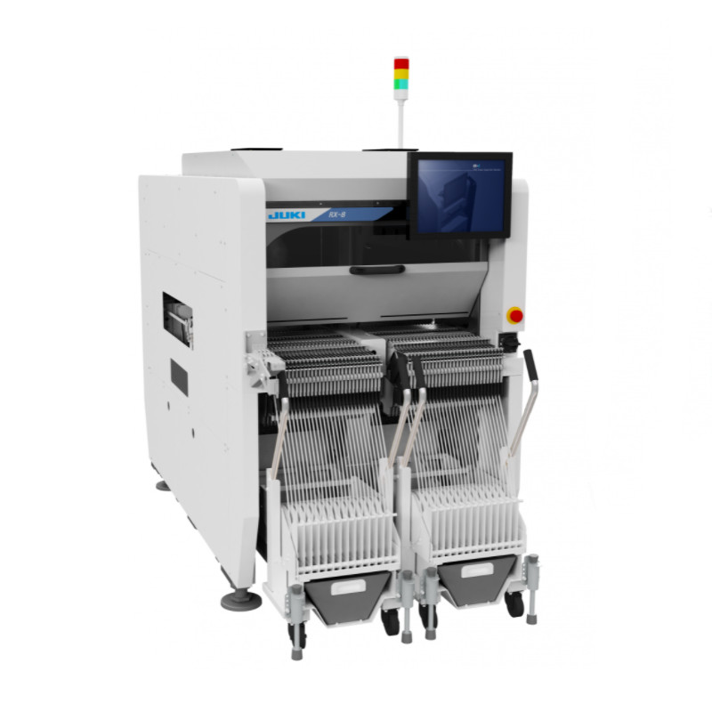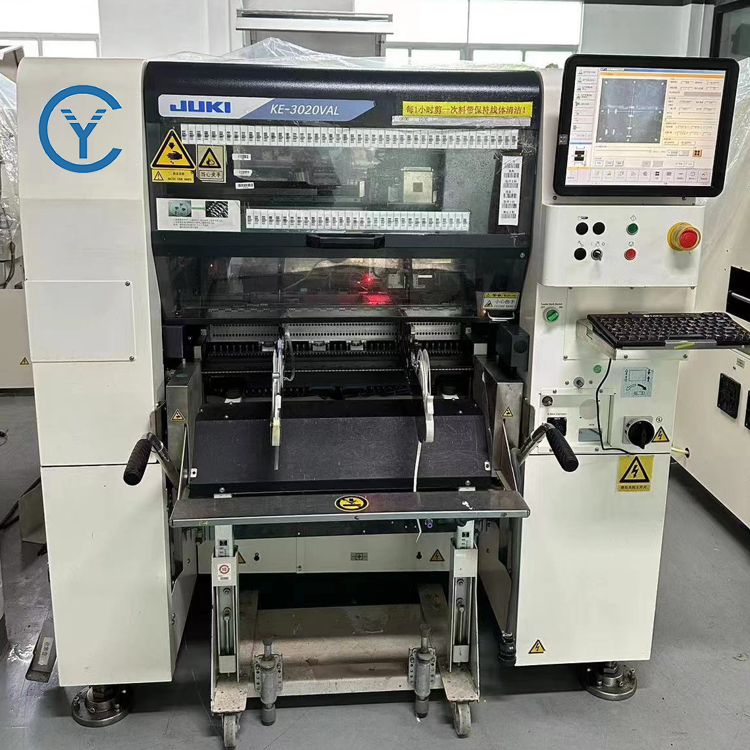
JUKI High-Speed Flexible Pick and Place Machine KE-3020VA
1.JUKI Basic Technology
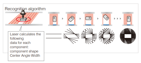
JUKI laser centering for flexibility and quality
The machine can recognize components of various shapes: from an ultra miniature components such as 0402 (01005) chips up to 33.5mm square components such as PLCCs, SOPs, BGAs, and QFPs. When the machine recognizes a component with laser, variations such as shape, color, and reflection do not matter.
2.High Productivity
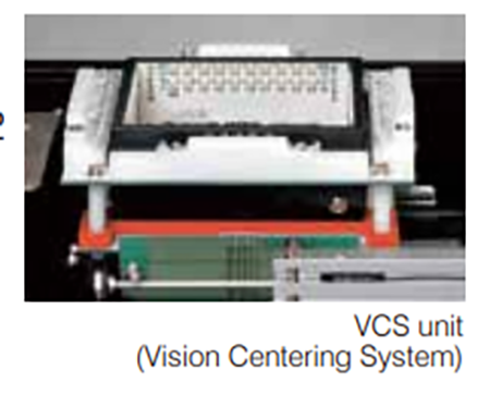
(1)High-speed, on-the-fly vision centering
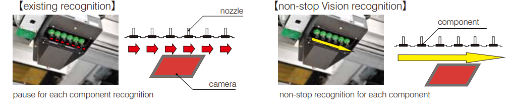
dual upward looking strobing cameras capture images in high speed for large, fine pitch, or odd-form compon-ents.
(2)Simultaneous on-the-fly component 2 centering for high-speed production
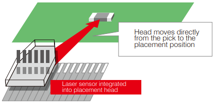
Laser sensor is integrated into the placement head for on-the-fly centering. Head moves directly from the pick position to the placement position for the shortest possible head travel and maximum place-ment speed.
(3)High-resolution Camera
Enable high-accurate inspection for components like QFP with lead pitch 0.2 mm.
3.High Flexibility
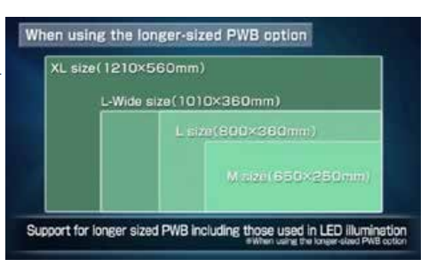
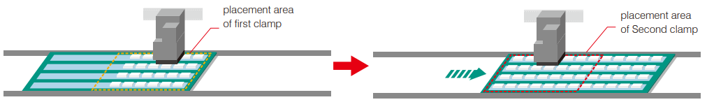
Capable of placing a longer board up to 650mm×250mm(M size), 800mm×360mm(L size), 1,010mm×360mm(L-wide size), 1,210mm× 560mm(XL size) by automatically indexing the board twice in each station. As a result, the production of a long PWB used for the LED lighting etc. is enabled.
k. ●Solder Recognition Lighting (option)
The solder print can be recognized as BOC mark when there is no BOC mark on the PWB or the circuit. When the twice-fed long PWB is transported, the placement pad etc. on which the solder print is performed at the placement of components in the range where the BOC mark is not prepared can be used as BOC mark
●Component Quantity Control (option)
The lot of the product (PWB) where the components (LED components etc.) are placed is managed. When a PWB is loaded, it is checked whether components required to complete a production of the PWB remain in the feeders with components in different lots not being mixed in a PWB. If components are not enough, a warning is displayed before the placement starts.
4.High Quality
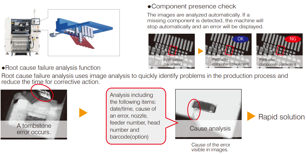
Prevention of defective PWBs and rapid analysis of the cause and corrective action Placement Monitor
An ultra miniature camera built into the head section captures images of component pick and placement in real time. An analysis is run for presence/absence and traceability information can be saved. This unique function prevents defective PWBs and reduces the time for root cause failure analysis.